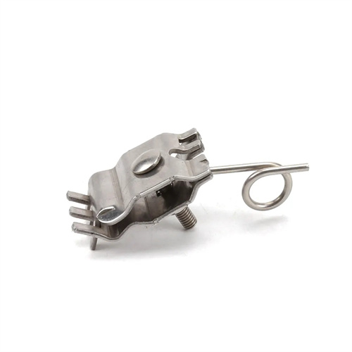
Copper and copper alloy flat strips for lead frames
Copper and copper alloy flat ribbon for leadframes is a key packaging material for integrated circuits and semiconductor devices. It connects the chip’s internal circuitry with external wiring and requires extremely high conductivity, excellent formability, and weldability, making it a core component in the electronics and information industry. Common materials include oxygen-free copper (TU1, TU2), phosphorus-deoxidized copper (TP2), copper-iron alloy (C19400), and copper-nickel-silicon alloy (C70250). TU1 flat ribbon has a conductivity of ≥101% IACS and is suitable for high-frequency chips. C19400, with an iron content of 2.0-2.8%, offers high strength (tensile strength ≥400 MPa) and a conductivity of ≥85% IACS, making it a general-purpose choice. C70250, with a nickel content of 2.0-3.0% and a silicon content of 0.4-0.8%, has a strength of ≥500 MPa and is suitable for high-power devices. The flat belt has a thickness of 0.05-0.3mm, a width of 5-50mm, a dimensional tolerance of ±0.002mm, a surface finish of Ra≤0.02μm, and edge burrs ≤0.005mm.
The production process for copper and copper alloy flat strip for lead frames represents the highest level of precision in copper processing, requiring complete control of purity and accuracy. First, ultra-high-purity electrolytic copper (99.99%) or alloy raw materials are smelted in a vacuum melting furnace, with an oxygen content controlled to ≤0.001% (for oxygen-free copper). The ingots are continuously cast with a cooling rate of ≥100°C/min to achieve fine grains (≤20μm). After hot rolling to a thickness of 1-3mm, they undergo multiple cold-rolling passes with a total reduction of ≥90% and a rolling speed of 50-100m/min to ensure grain refinement and a uniform texture. Intermediate annealing is performed under hydrogen protection (temperature 300-400°C) to eliminate work hardening and prevent oxidation. Finish rolling is performed using a 20-high mill, with a thickness tolerance of ±0.001mm and a surface roughness Ra ≤0.01μm. The finished products are slit (edge verticality ≤ 0.01mm), cleaned, and then pass the conductivity test (≥85% IACS) and the bend test (180° no cracks) to ensure that they meet quality standards.
In integrated circuit packaging, copper alloy flat tape for leadframes serves as the “bridge” connecting the chip to the outside world. CPU chip leadframes utilize C70250 flat tape, 0.1-0.2mm thick. Hundreds of pins are precision-stamped, with a pitch of ≤0.2mm. This has helped one chip manufacturer achieve a 99.2% packaging yield. Memory chips (such as DRAM) utilize C19400 flat tape, which boasts a conductivity of ≥85% IACS and excellent heat dissipation. This has reduced the operating temperature of one memory company’s chips by 5°C. Power semiconductors (such as IGBTs) utilize TU2 flat tape, 0.2-0.3mm thick, capable of handling high currents (≥100A). This has resulted in a 30% improvement in device reliability for one power electronics company.
Demand for leadframe flat tape continues to grow in the consumer and automotive electronics sectors. Smartphone processors utilize 0.05-0.1mm thick C70250 flat tape, which has over 1,000 pins. This has reduced the chip package size of one mobile phone brand by 30%. Automotive MCU (microcontroller unit) leadframes utilize C19400 flat tape, which boasts a temperature resistance of 150°C and is suitable for engine compartment environments. This has reduced the failure rate of one automaker’s electronic control system by 40%. Smart home sensor chips utilize TP2 flat tape, offering reasonable cost and stable performance. This has improved the price/performance ratio of one sensor manufacturer’s products by 20%.
As chip packaging evolves toward higher density and miniaturization, copper alloy flat ribbon for lead frames continues to achieve breakthroughs in performance. Manufacturers have developed ultra-thin flat ribbon (thickness ≤ 0.03mm) for 3D stacked packaging, increasing chip integration by 50% for a semiconductor company. To meet the high-frequency demands of 5G chips, a low-loss copper alloy flat ribbon (C18150) with a conductivity ≥90% IACS has been developed, reducing signal transmission loss by 10% and improving product performance by 15% for a communications chip manufacturer. Using atomic layer deposition technology, a nanoscale protective layer forms on the ribbon’s surface, increasing corrosion resistance by 100% and extending its storage life to two years at a packaging facility. In the future, with the advancement of artificial intelligence and the Internet of Things, copper and copper alloy flat ribbon for lead frames will continue to develop towards higher strength (≥600MPa) and higher conductivity (≥95% IACS), supporting continued breakthroughs in chip technology.